This is the circuit diagram of 6V to 12V DC to DC voltage converter (6V to 12V DC voltage doubler). This is the active circuit for voltage doubling from 6 volt to 12 volt DC with 1A maximum current. The IC is used as switcher device.
Schematic diagram:

Components and its usage:
| IC | Switcher/regulator | LM2577T-ADJ (Texas Instrument) |
| R1 and R2 | Voltage devider for monitoring output voltage | 20Kohms pot. (Bourns) |
| Cin | Decoupling | 0.1?F, 63V MKS condensator (WIMA) |
| L | Use a good quality coil! | 160?H toro?d (2.5A, 70mohms, nickel-iron core) |
| D | Current higher than output current! | FR603 60V reverse breakdown, 3A Schottky-diode |
| Rc and Cc | Pole-zero compensation network | 2200ohms, 5% and 1?F, 63V elco (Philips) |
| Cout | Get a low ESR type! | 2200?F, 16V elco (Telecon) |
6V to 12V DC to DC voltage converter circuit works:
When the switch is closed an extra current flows through the inductance and stores energy there. The capacitor supplies the load with current during this time.
After the switch closes the capacitor is charged by the energy stored in the inductance and an extra current starts flowing through the load, causing the output voltage to rise (energy is supplied directly from the input source also as long as the diode is forward biased). During this time, the system behaves like a RLC-circuit, so, after a while, the current decreases. The switch is then closed again and the cycle repeats. One could say that charge is pumped from input to output, increasing the output voltage up to the point where there is an equilibrium between the discharging of the capacitor while the switch is closed and the charging by the inductor while the switch is open.
PCB layout:
This is the simple and easy built of PCB design layout for above 6V to 12V DC Voltage converter diagram.
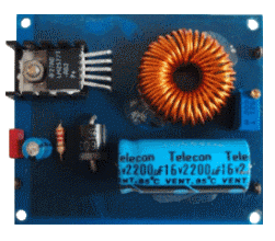
The circuit will look like following image:


